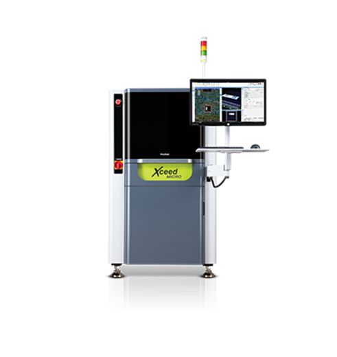
Xceed-MICRO
Ultra-Precision 3D AOI for Semiconductor Packaging
Description

PARMI’s ultra-precision 3D AOI solution is designed for the demanding inspection requirements of advanced semiconductor packaging. Its high-resolution laser line scanning technology delivers fast, accurate, and repeatable 3D measurements of extremely small and complex features.
The system provides reliable inspection even on highly reflective surfaces and maintains stable measurement performance regardless of color, material, or surface roughness. This enables precise quality control across a wide range of semiconductor packaging processes and applications.
By detecting dimensional deviations, material defects, and process irregularities at an early stage, the system helps improve yield, strengthen process control, and ensure consistent product quality.
Key benefits:
- Ultra-precise 3D inspection for semiconductor packaging
- Extremely fast, high-resolution laser line scanning
- Reliable inspection of highly reflective surfaces
- Stable measurement regardless of color, material, or surface roughness
- Accurate inspection of very small and complex features
- Early detection of process and material deviations
- Improved process control and production yield
- Consistent and repeatable inspection results
Inspection applications:
System-in-Package (SiP), die attach, underfill, solder paste, solder bumps, copper clips on die, IGBT modules, and other advanced semiconductor packaging applications.